
Researchers hope to lower the costs and barriers to advanced manufacturing with a new chiplet-filled ink that can be printed into integrated systems.
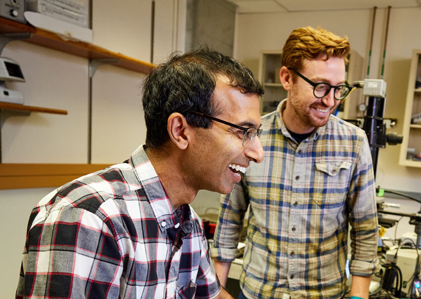
Under a microscope, they look like ants. Tiny black rectangles scurrying about, twitching back and forth and then settling into precise alignment, as if headed for a picnic. In truth, each of those twitching dots is a computer chip — a “chiplet,” as Eugene Chow, the project leader, likes to call them. The patterns they form represent a new way to create computer circuits — not composed of one large computer chip but many small chiplets, guided into place with electrostatic forces.
“It’s electronic ink,” says Chow, who has nurtured the technology development over the last decade, along with his partner Jeng Ping Lu and several others. “The individual chips can perform any number of functions — memory, display, logic, communications, sensing, and so forth — and we can tell them each exactly where to go and then link them together to form circuits.”
Chow calls the process software-controlled microassembly, and it represents a transformation in assembly technology. Currently, software-controlled assembly, where engineers can readily manipulate where each individual building block goes within an integrated system, is limited to large objects — a millimeter or larger — that can be controlled by robotic assembly methods. Microassembly of objects smaller than a millimeter, on the other hand, requires methods that cannot be controlled by software, using techniques from chemistry, fluidics, or biology-like self-assembly to produce circuits. They are extremely challenging to design.
Chow’s new process is potentially a fundamental new way to address the broad challenge of building scalable, heterogeneous microsystems. If fully realized, the new process could transform how displays, electronics, and eventually even materials are built. A single present-day nanofabrication facility — or a fab, as they are known in the semiconductor field — can cost billions to build. Developing new chips is slow, restricted to a handful of the biggest players, and prohibitively expensive.
Currently, displays or electronics are built with expensive monolithic processes, essentially as thin films on one large chip, which are limited to high-volume applications with limited materials and device diversity — and zero customizability.
Radically different approach
Chow envisions something new — microassembly facilities costing an order of magnitude (or two) less to build — millions rather than billions of dollars.
The reduced cost alone could have a democratizing effect on electronics, bringing innovative but underresourced new players to the field. Add in the speed and ease with which microassemblers can create new and radically different circuits combining a variety of devices, and the microassembler represents a fundamental shift in fab and design that frees both wallets and minds to pursue previously unimaginable possibilities.
New ideas and prototype circuits could be designed and printed in a lab at will by changing a few lines of code. Entire production facilities might fill a lab, not a city block. Low-volume, customized products could be built affordably.
“The iterative advantages would be profound,” Chow says. “We could rapidly print anything a designer can imagine by leveraging large libraries of chiplets, potentially enabling new technologies to get into systems decades earlier than conventional approaches.”
Theoretically, any semiconductor device or material from industry or academia could be used in a chiplet ink, bringing the best current existing chiplet device technologies to the market. This is in stark contrast to other fabrication approaches, which depend on new, risky materials that are hard to monolithically integrate, especially into large area modern fab tools.
Printing circuits
Imagining their chiplet-like particles could be suspended in ink and printed was a key insight for Chow and his team. Needing a way to control and arrange chips precisely and then to wire them together into circuits, the researchers learned to manipulate fine-scale electrostatic force fields with software to achieve precise, directed assembly.
“Using these software-controlled force fields, we can tell the chiplets exactly where to go. When they find their intended spot, they stop and settle precisely into place,” said Chow. Using the same techniques, the researchers can repair (or heal) misplaced assemblies and assemble different types of chiplets in one step. The assembled pattern of chiplets is then transferred to a substrate and interconnected into the system.
The electrostatic approach and planned high-throughput system architectures, key for practical applications, are inspired by laser printer concepts. The laser printer was invented at PARC, where Chow and Lu have worked for over 20 years. PARC is excited to continue to drive advanced manufacturing research at SRI.
“Ultimately, microassembly printers have the potential to be a disruptive new manufacturing tool for next generation displays, electronics, and materials. SRI has an amazing breadth of interdisciplinary talent which can help to realize this vision,” says Chow.