
SRI’s work on DARPA’s HAPPI program seeks to measurably advance the capability of circuits that transmit information using light rather than electrons.
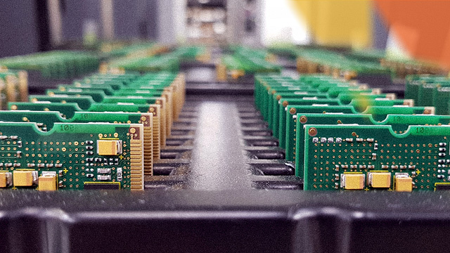
All integrated circuits used in computing share a fundamental dynamic: When they become dense and connection-rich, they become more powerful, but they also generate more heat. At some point, they reach a limit where the heat generated begins to degrade the performance of the circuit.
Over the past two decades, scientists have sought to address these limitations by advancing photonic integrated circuits (PICs). Today, our standard circuits rely on semiconductor-based chips and metal connectors to transmit information using electricity. PICs, instead, use light. Theoretically, PICs can attain unprecedented routing density, given that light produces much less heat than electricity. In practice, scientists need to more precisely control light within an integrated circuit before PICs can achieve their full potential and advance the next generation of information processing.
SRI researchers recently began working on a Defense Advanced Research Projects Agency (DARPA) program called Heterogeneous Adaptively Produced Photonic Interfaces (HAPPI) that aims to significantly advance the capabilities of photonic circuits.
“SRI’s Boulder facility has incredible expertise in designing and testing PICs,” says SRI senior research scientist David Hill. “At our Princeton facility, we specialize in doing all sorts of unique fabrication — things that fall outside of the standard offerings of a conventional foundry service.” These facilities and capabilities, he notes, have made SRI a leader in next-generation photonics research.
The challenge of advanced photonic circuits
“In electronics, the industry has spent many decades developing this whole metallization back-end,” Hill observes. “It’s stacks and stacks of different layers of metal that help to connect different areas on a chip that couldn’t be connected in a purely two-dimensional way. You keep getting more and more density in terms of connections, memory, and storage. That’s really what enables the modern CMOS chip, and that level of complexity does not yet exist for photonic integrated circuits.”
“I don’t want to say that photonic computing will replace all electronic computing. But there are particular cases where PICs hold major advantages over traditional electronics.” — David Hill
Achieving a complex three-dimensional photonic circuit, he points out, requires solving three fundamental challenges: Turning light out of the two-dimensional plane in the first place, then getting light to propagate through the entire thickness of a wafer so that it can move between chips, and finally ensuring low loss transfer of light between chips, especially in cases where there is misalignment between those chips.
DARPA’s HAPPI program aims to improve multiple specific performance metrics of PICs related to low-loss interconnects and high photonic routing density. SRI’s work will be split into two phases: first creating a proof-of-concept for a PIC with four photonic layers, and then further boosting the density of the circuit configuration. Critical enablers of SRI’s approach will include new approaches to etching vertical wave guides, designing turning mirrors, and employing polymer-based interconnects.
The benefits of PICs: national security and beyond
Advanced photonic integrated circuits have profound implications for national defense, given the reliance of modern military technologies on powerful, compact, energy efficient integrated circuits. But PICs also have commercial implications in cases where today’s electronic circuits are running up against physical limits.
Hill points to the imaging space as one area where photonic circuits might lead to fundamental breakthroughs. Today’s circuits can’t support the high data collection rates (sometimes more than 1,000 frames per second) of high-performance imagers. PICs would theoretically be able to transmit that data with high fidelity, or else rapidly “prune” (simplify) the data prior to transmission by rapidly weeding out unnecessary information.
Making the innovations of the HAPPI program scalable isn’t just about raw capabilities, Hill adds. The team is also thinking about the eventual large-scale rollout of PICs: “These tools need to be compatible with foundry processes in the future — that’s an underlying design constraint.”
“I don’t want to say that photonic computing will replace all electronic computing,” Hill concludes. “But there are particular cases where PICs hold major advantages over traditional electronics.”
Contact us to learn more about our foundry services and other capabilities on the cutting edge of computing.