The 75 Years of Innovation series highlights the groundbreaking innovations spanning from SRI’s founding in 1946 to today. Each week, SRI will release an innovation, leading up to its 75th anniversary in November 2021.
Development of a faster, less power-hungry version of a metal oxide semiconductor
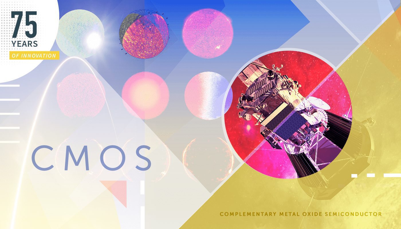
A historic moment in semiconductor development: The CMOS (complementary metal-oxide-semiconductor)
In 1965 two interesting and interrelated events happened that would lead to the digital technology we use today. First, Intel co-founder Gordon Moore expressed an idea that came to be known as Moore’s Law, saying that the number of transistors contained in an integrated circuit — and therefore, the circuit’s computational power — would double every two years.
The result of this doubling of power has meant that computers have increased in performance and decreased in cost ever since. Maintaining this pace, however, required continual technological advances, and a significant leap in semiconductor integrated circuit technology came with the development of the complementary metal-oxide-semiconductor or CMOS.
CMOS was a product of the innovators at the David Sarnoff Research Center, now part of SRI International. CMOS technology is widely used across microprocessor manufacturing, integrated into most of the world’s electronic circuitry. Here’s how CMOS increased processing speed while requiring less power.
Powering down — how CMOS made computers faster with less power
Before CMOS, bipolar transistor technology was the norm. Although this older technology enabled fast-switching circuits, it was relatively power-hungry, making battery operation problematic. For electronics, power-hungry is to be avoided. CMOS revolutionized electronics by changing the metrics of power vs. speed. Today, CMOS circuits are used widely in electronic components such as microprocessors and mobile imaging sensors.
In the 1970s, microprocessors initially used NMOS technology, which stands for n-type metal-oxide-semiconductor. NMOS used only negative (n-type) charges in integrated circuit logic gates. While NMOS circuits were fast and powerful, they were power-hungry. CMOS uses complementary, symmetrical negative (n-type) and positive (p-type) charges in logic gates, reducing a circuit’s energy consumption while maintaining its speed.
CMOS was originally developed in 1965 as part of a circuit design program for the Air Force. It was developed by Gerald Herzog and his team at the David Sarnoff Research Center (now part of SRI). Out of this work, Herzog and his team created a 288-bit static memory integrated circuit. This early development of metal oxide semiconductors was a part of the continuing push to smaller-sized electronics with lower power needs that have allowed the development of today’s portable devices. The superior low power consumption of CMOS circuits allowed for higher chip density with a lower power draw, making the chips more efficient and more powerful, allowing for Moore’s Law to come to fruition.
The many and varied applications of CMOS
CMOS are used in many varied applications. Two examples from the SRI portfolio include:
NASA’s Parker Solar Probe
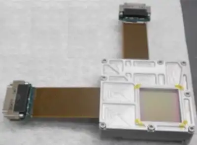
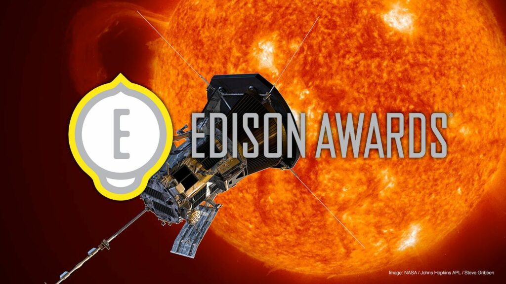
Launched on August 12, 2018, the Parker Solar Probe is used to study the dynamic region close to the sun. SRI International used CMOS technology and SRI innovations in imaging onboard the Parker Solar Probe. The probe’s imaging instrument is a wide-field imager for solar probe (WISPR), developed by the U.S. Naval Research Laboratory. This instrument contains two coronagraph telescopes that use SRI’s active-pixel CMOS detectors. These CMOS sensors capture high-resolution images of the sun’s atmosphere, including coronal mass ejections and solar wind. In 2020, SRI International was awarded an Edison Award for technology innovation for this project.
Low-light NV-CMOS image sensors for day and night imaging
SRI International has vast experience in developing imaging technologies, and CMOS has played an important part in extending the boundaries of imaging techniques. SRI recently developed a new type of CMOS known as NV-CMOS™; the NV stands for “Night Vision.” NV-CMOS image sensor technology can capture images over the full range of illumination from bright sunlight to starlight. In 2019, SRI began developing a digital night-vision camera to support the U.S. Army’s IVAS (Integrated Visual Augmentation System) program. This project was based on a low-light-level NV-CMOS imager integrated into a custom camera module optimized for low size, weight and power (SWAP).
Technological development is like a cascade; one thing leads to another, which leads to another, and so on. CMOS technology paved the way for low-power, high-speed microprocessors, providing a springboard for other innovations. The miniaturization and power-reduction of CMOS opened the door for a wide variety of technologies, facilitating progressive imaging without which we would not have the types of devices that define our modern world.
Learn more about our innovations in space and security.
Resources
Intel Museum, Gordon Moore: https://www.intel.co.uk/content/www/uk/en/history/museum-gordon-moore-law.html
NASA Parker Solar Probe https://www.sri.com/hoi/nasa-parker-solar-probe/
CMOS integrated circuit- https://www.sri.com/hoi/cmos-integrated-circuit/
Exploring the solar system with SRI’s CMOS Imager
Low-light CMOS sensors: https://www.sri.com/publication/low-light-nv-cmos-image-sensors-for-day-night-imaging/
Parker Solar Probe – Edison award: https://www.sri.com/press-release/parker-solar-probe-edison-award/